Microsoft Says AI Is Making Chip Design Easier — But Engineers Aren’t Going Anywhere
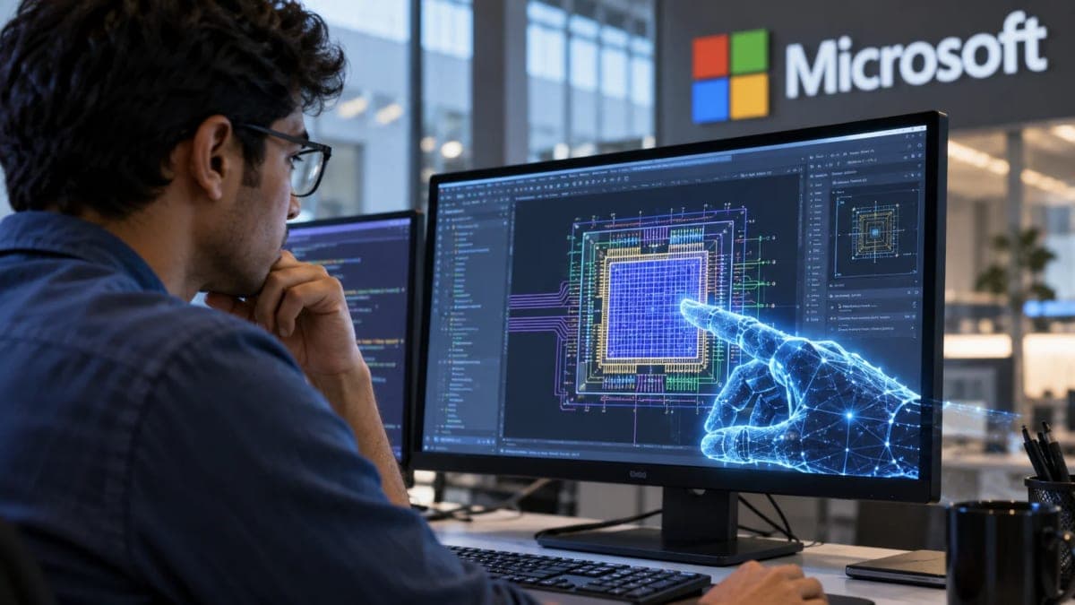
Microsoft has shown how artificial intelligence could make chip design easier to get into, using its Discovery platform to help an engineer with little semiconductor-design experience take a simple processor from an initial idea to a physical chip layout.
The experiment, published by Microsoft on September 17, used Microsoft Discovery, the company’s AI platform for scientific and engineering work. The project centred on a RISC-V processor core connected to a small matrix-multiplication accelerator designed for a low-power embedded device.
At first glance, it sounds like another example of AI learning to do the work of highly trained engineers. But that isn't really what Microsoft demonstrated.
The AI didn't independently design a cutting-edge processor, nor did it produce a commercial chip ready to send to a factory. Instead, Discovery acted more like an engineering assistant, helping someone unfamiliar with chip design work through a complicated process that normally takes considerable specialist knowledge to navigate.
That may be less dramatic than saying “AI designed a chip,” but it is also closer to what actually happened — and potentially more important in the long run.
From an idea to a physical chip layout
The engineer behind Microsoft's experiment came from a satellite-engineering background rather than professional semiconductor design.
With help from Discovery, the engineer worked through several stages that are part of a real digital chip-development process.
The project started with a specification for a RISC-V processor core connected to a matrix-multiplication accelerator. The design then moved through C code and high-level synthesis, or HLS C, before being translated into register-transfer-level logic.
Verilog was used at the RTL stage to describe the digital hardware.
The project eventually reached physical implementation using OpenROAD, an open-source electronic design automation, or EDA, flow. Microsoft also used the openly available SKY130 process environment instead of a cutting-edge semiconductor manufacturing technology.
That's an important detail.
Microsoft wasn't trying to build a processor capable of competing with the latest chips from Nvidia, AMD, Intel, Qualcomm or Apple. The company describes the project itself as small and based on limited instructions, using a manufacturing process far removed from today's most advanced semiconductor nodes.
Even so, getting from an initial specification to a physical layout is a much more involved exercise than simply asking an AI chatbot to generate some Verilog code.
The engineer still had to move through several layers of the chip-development process, and Discovery helped make those steps easier to understand and manage.
So what did the AI actually do?
Discovery didn't replace the chip-design software. It worked alongside it.
That's probably the easiest way to understand Microsoft's experiment.
Discovery combines large language models with specialised AI agents and orchestration tools. The idea is that researchers can describe what they are trying to achieve in natural language while the system helps organise information, software tools, simulations and computing resources around the task.
During the chip project, the engineer used that natural-language interaction to work through different stages of the design.
After generating a physical layout, the experiment moved into optimisation. Parameters such as the target clock speed could be changed and tested, allowing different versions of the design to be explored without manually managing every step.
This is where AI could become particularly useful in semiconductor engineering.
Chip designers constantly have to balance competing priorities. A design may need to run faster, consume less power, occupy less physical space or meet strict timing requirements. Improving one area can create problems somewhere else.
That means engineers often have to explore many possible configurations before finding a design that meets their requirements.
AI agents connected to established EDA tools could potentially run more of those experiments, examine the results and help engineers identify which design directions deserve further attention.
Microsoft is already exploring this idea with Synopsys, one of the major companies behind professional chip-design software. Synopsys has said that multi-agent workflows using Microsoft Discovery could help engineering teams deal with increasingly complicated chip designs and a shortage of specialised talent.
Making chip design easier doesn't make chip designers unnecessary
This is also where the limits of Microsoft's demonstration become important.
The experiment does not mean someone can describe a processor in a few sentences and have AI deliver a commercially competitive chip ready for manufacturing.
Microsoft's own engineer acknowledged that the resulting design wouldn't match what an experienced chip designer could produce.
Professor Nan Wu, whose comments were included in Microsoft's account of the project, made a similar distinction.
Wu said systems such as Discovery could “significantly lower the barrier to hardware design” by providing natural-language assistance and making rapid exploration easier. But specialist knowledge is still needed to understand the results produced by EDA tools and optimise a design for its intended application.
In other words, AI may help people start experimenting with hardware without knowing every part of the process beforehand.
That's very different from replacing semiconductor engineers.
Why making chips isn't like writing software
Generative AI has already made software development much more accessible.
Someone can now describe a basic application to an AI coding assistant and get usable code within minutes. Developers also have access to enormous open-source ecosystems, inexpensive cloud infrastructure and mature development tools.
Hardware comes with a different set of problems.
A processor has to move through architecture, logic design, verification, timing analysis, placement, routing, power analysis and other stages before it can even approach manufacturing.
And a design that works in a simulation isn't automatically ready to become a physical product.
Manufacturing introduces another layer of requirements, including fabrication rules, verification, packaging, testing and cost. Advanced chips also depend on specialised process-design kits and intellectual property that aren't freely available in the way many software libraries are.
Microsoft's experiment avoids some of those obstacles by relying on open-source tools and an accessible process technology.
That makes the project particularly useful as a demonstration of how AI could help with learning, prototyping and experimentation.
It does not make it a demonstration of AI building a leading-edge processor.
Discovery is becoming more than a research assistant
The chip project also gives a clearer picture of what Microsoft wants Discovery to become.
Microsoft made Discovery generally available earlier this year and also introduced a desktop version in preview. The platform brings together AI agents, scientific reasoning, knowledge systems and high-performance computing.
Microsoft is targeting areas including materials science, life sciences, semiconductors, energy, manufacturing and advanced engineering.
A major part of the idea is making natural language an easier way into these specialised workflows.
Researchers don't necessarily have to learn every platform-specific command or API before they can begin exploring a problem. They can describe their goal conversationally, while AI agents help coordinate some of the technical work behind it.
Microsoft says its Discovery desktop app is intended to make that starting point even easier for researchers, students and smaller teams. It can also be used with a GitHub Copilot account.
This reflects a broader change in how companies are thinking about generative AI.
The focus is gradually moving beyond chatbots that simply answer questions. Increasingly, AI models are being connected to specialist software and given the ability to work across several tools to complete more complicated tasks.
Chip design is a particularly interesting test because engineers already rely heavily on sophisticated software.
The bigger opportunity could be speed
For the semiconductor industry, the most useful outcome may not be turning beginners into chip designers.
It could be helping experienced engineers explore far more possibilities in the same amount of time.
A chip engineer can only manually investigate so many design variations. Simulations, implementation runs and analysis all take time, especially as designs become larger and more complicated.
AI agents could potentially run more experiments, compare the results and use what they learn to decide which variations should be tested next.
Microsoft says Discovery is designed around this kind of cycle: propose an idea, test it with specialised tools, analyse what happened and use the results to guide the next attempt.
That could become increasingly valuable as semiconductor designs grow more complex.
Microsoft also has a direct reason to care about the problem.
The company now designs custom processors for its Azure data centres, including its Maia AI accelerators and Cobalt server CPUs. It has increasingly talked about designing silicon, networking, memory, software and power infrastructure together as it tries to make large AI systems more efficient.
So Microsoft's interest in AI-assisted chip engineering isn't purely academic. It sits alongside the company's much larger push into custom hardware.
What the experiment actually tells us
Calling Microsoft's project an example of “AI designing a chip” would be tempting, but it misses the most interesting part of the story.
The AI helped an engineer without deep semiconductor-design experience work through a genuine hardware-development workflow using established programming languages, EDA software and an accessible process technology.
That's a meaningful difference.
Hardware has traditionally been much harder to experiment with than software. If AI can explain unfamiliar steps, help generate intermediate designs, connect different engineering tools and make technical feedback easier to understand, researchers may be able to test hardware ideas without needing years of semiconductor experience just to get started.
There is still a large gap between that and building a commercial chip.
Producing a physical layout is one milestone. Creating a highly optimised design, verifying that it works correctly, ensuring it can actually be manufactured and turning it into a competitive product is another challenge altogether.
Microsoft's experiment doesn't close that gap.
What it does show is that AI could make the starting line easier to reach.
And if these systems continue improving, the bigger change may not be that AI replaces chip designers. It may be that engineers can spend less time wrestling with the mechanics of complicated design workflows and more time deciding what hardware they actually want to build.